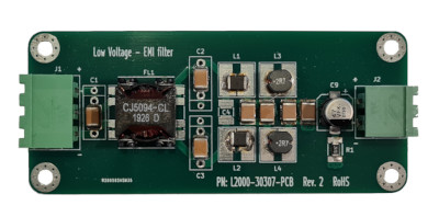
EMC Filter PCB - Low Voltage
No matter how good your PCB layout would be, you are going to have stray capacitance and inductance. Because of that, the energy associated with voltage and current transients will couple with other traces. This will reflect in having unwanted noise on other traces.
Good PCB design, to guaranty that the end product, will comply with the EMC (ElectroMagnetic Interference) standards such as the CISPR 14, CISPR 32, must limit the energy associated to the noise that goes out from the system. This energy, while described by the Maxwell's equations, are divided in two types, conducted and radiated noise. In this article, it will be presented a filter you can add before your system to limit the conducted noise energy that goes out from the system or try to enter into it. The project is a general purpose PCB that can be used to design an ad-hoc filter.
MSP430 Step by Step - Capitolo V
Dopo essere diventati degli esperti relativamente all’architettura MSP430 e agli strumenti necessari per iniziare la programmazione e sviluppo di applicazioni contenenti questi microcontrollori, iniziamo a programmare! Come ogni buon programmatore ben educato, iniziamo con il salutare il mondo. Un programma semplice ed essenziale che ci permetterà di compilare il nostro primo programma e vedere i primi risultati.
Scheda di sviluppo P32Board
La scheda di sviluppo P32Board è un sistema completo che permette di sviluppare molte applicazioni con la famiglia di microcontrollori PIC32MZ, senza richiedere l’aggiunta di hardware esterno. In particolare, possono essere sviluppate applicazioni con display LCD 16x2, applicazioni con protocollo SPI, I2C, UART e applicazioni con ingressi analogici o digitali. In aggiunta, è possibile connettere qualsiasi hardware esterno grazie ai connettori di espansione. La compatibilità della scheda con i programmatori e i debugger di casa Microchip la rendono inoltre integrabile nel sistema di sviluppo MPLAB X.
Autore: Ivo Colleoni

3D printed PCB assembly test fixture
The design phase is the most important part within a new product development cycle. Investing enough time on it, is fundamental for good quality products. Nevertheless spending enough time in testing a new system is also as much important as the design phase. Only by testing a real system is possible to properly validate how the integration of the sub-modules are affecting each other. Last but not least, during the test phase it is possible to check how the system usability is. In this article it will be presented a 3D printed fixture to test new assembled PCBs that come back on our desk. The fixture has been designed to be flexible enough and be used in various scenarios enabling a quick PCB Assembly (PCBA) test and replacement.

Dallo schema elettrico al PCB
Realizzare un sistema elettronico, necessita il passaggio per varie fasi e un certo numero di iterazioni al fine di rendere il progetto finale quanto più funzionale possibile. Le varie fasi possono variare a seconda dell’applicazione e soprattutto se il progetto debba essere catalogato come “Maker” o “professionale”. Frequentemente in sistemi Maker, non ci si preoccupa molto della fase progettuale e si pone ad essa poco tempo. La realizzazione è spesso anche fatta velocemente al fine di realizzare pezzi unici. Quando si voglia realizzare un sistema professionale le cose cambiano. La fase progettuale diventa una fase importante della progettazione come anche la fase di test del sistema, al fine di verificare che le specifiche di progetto siano rispettate.

Registrati al sito
Accedi a tutte le risorse e articoli non visibili pubblicamente, puoi registrarti con pochi passi.
Login
Online
Abbiamo 768 ospiti e nessun utente online