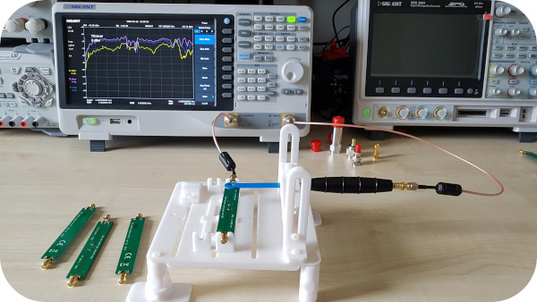
PCB Layout - understand stray capacitance and inductance
The PCB board layout is the last challenge after having designed the schematic. While things may work on sub-modules level, once all the system gets assembled on the PCB, additional problems may occur. Several “Tips and Tricks Cookbooks” are providing recommendations to the designer making the PCB layout the right way. Nevertheless properly understanding the limitation and boundary conditions at which a certain rule can be used, is fundamental. Thus, in this article, rather than talking about “Tips and Tricks” we will go down to the details of understanding from where the stray capacitance and inductance come from. Indeed, the two are responsible of the major problems a wrong layout may cause at system level.

