PCB Layout - PCB ground layer considerations
Old system assemblies, based on vacuum tubes, were often made directly on the manufacturing floor without any PCB support. With the increased signal frequency and system integration, made possible by transistors and ICs, using a PCB was a must. Nevertheless, till the 80’, regulations were not covering commercial products as they do today. EMC (Electromagnetic Compatibility) and immunity tests are today part of the system requirements that may challenge the designer during the design phase. High-speed applications, precision analog, and the regulations that the system must fulfill, make the PCB a fundamental part of the design puzzle. In this article, we will take a closer look at the PCB ground layer. Using it is very important, but sometimes it could lead to more problems than benefits...
PCB Layout - understand stray capacitance and inductance
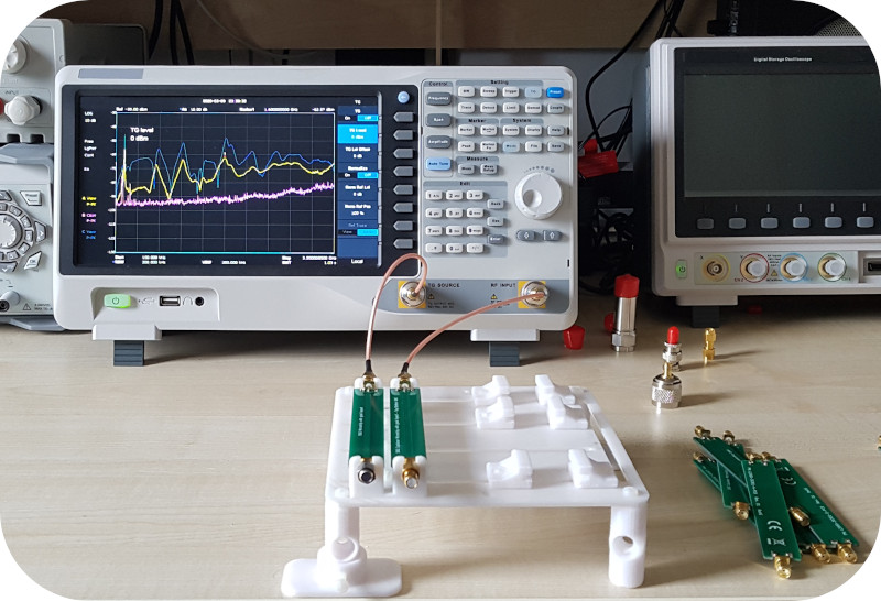
The PCB board layout is the last challenge after having designed the schematic. While things may work on sub-modules level, once all the system gets assembled on the PCB, additional problems may occur. Several “Tips and Tricks Cookbooks” are providing recommendations to the designer making the PCB layout the right way. Nevertheless properly understanding the limitation and boundary conditions at which a certain rule can be used, is fundamental. Thus, in this article, rather than talking about “Tips and Tricks” we will go down to the details of understanding from where the stray capacitance and inductance come from. Indeed, the two are responsible of the major problems a wrong layout may cause at system level.
EMC Testing - PCB layout and noise coupling
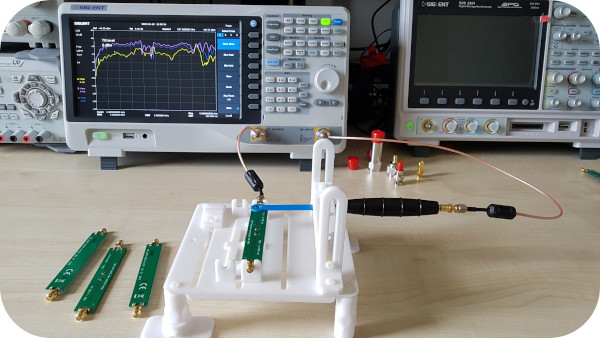
Engineers do not get surprised by hearing that for precision or RF applications, the PCB must be considered as an electronic component part of the system itself. Each trace routed on the PCB is part of the signal chain and must be carefully designed. This perspective should be actually taken beyond the precision and RF applications, indeed stringent regulations, such as the CISPR standards, apply to any electronic system. CISPR standards cover automotive, industrial and commercial systems and are used by different countries, such as Europe and US, as basis to validate the conformity of a certain electronic system from EMC (Electromagnetic Compatibility) perspective. In this article it will be shown how different trace layouts made on a standard FR4 PCB, may drastically affect the system radiation that may compromise the end product certification, either from conducted or radiated tests perspective. The article will highlights how a PCB should be carefully designed as part of the system, whatever the application would be, to make sure that you achieve the right performances but also you will comply with the EMC standards required for the FCC and CE marking.
Utilizzo del pulsante in applicazioni Embedded
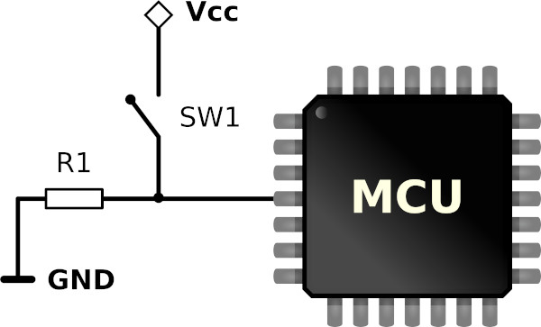
I sistemi embedded fanno spesso uso dei pulsanti come semplice interfaccia di input del sistema. L’utente tramite la pressione di un pulsante può facilmente cambiare lo stato del sistema, come accenderlo o spegnerlo, o inserire particolari dati. Il suo utilizzo è piuttosto semplice, tanto che sullo schema elettrico si pone poca attenzione su possibili malfunzionamenti. Un sistema robusto si differenzia sempre dall’attenzione che si pone ad ogni singolo componente e la verifica della compatibilità dello stesso con il sistema e le specifiche che devono essere soddisfatte. In questo tutorial si analizzerà prima lo schema elettrico base per collegare un pulsante, analizzando diverse possibili soluzioni. Verranno poi discusse le considerazioni che possono favorire l’una o l’altra soluzione. I componenti utilizzati saranno analizzati nel dettaglio al fine di garantire il corretto funzionamento del pulsante e del sistema che si sta progettando.
Conducted noise - Differential and Common mode noise
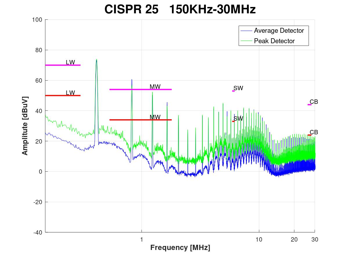
On the previous article we have seen what the conducted noise is and how it links with the radiated noise to. CISPR regulations require that you have two tests setup for testing conducted and radiated noise. In regards to the conducted noise, while the standards require that the absolute value should be below a certain threshold, understanding what contributes to the total noise, could be beneficial for the design. Indeed the conducted noise is made of two components, Differential Mode (DM) and Common Mode (CM). The two components summed together is what we measure with the spectrum analyzer or the receiver. In this article we see the details of the DM and CM. Out of the values the designer can better leverage how to dimension the EMI filter, either for the DM or CM noise.
Registrati al sito
Accedi a tutte le risorse e articoli non visibili pubblicamente, puoi registrarti con pochi passi.
Login
Online
Abbiamo 782 ospiti e nessun utente online


